PRODUCTS
- Home
- Products
- CPO Application
- Laser Die Eutectic Bonding System
CPO Application
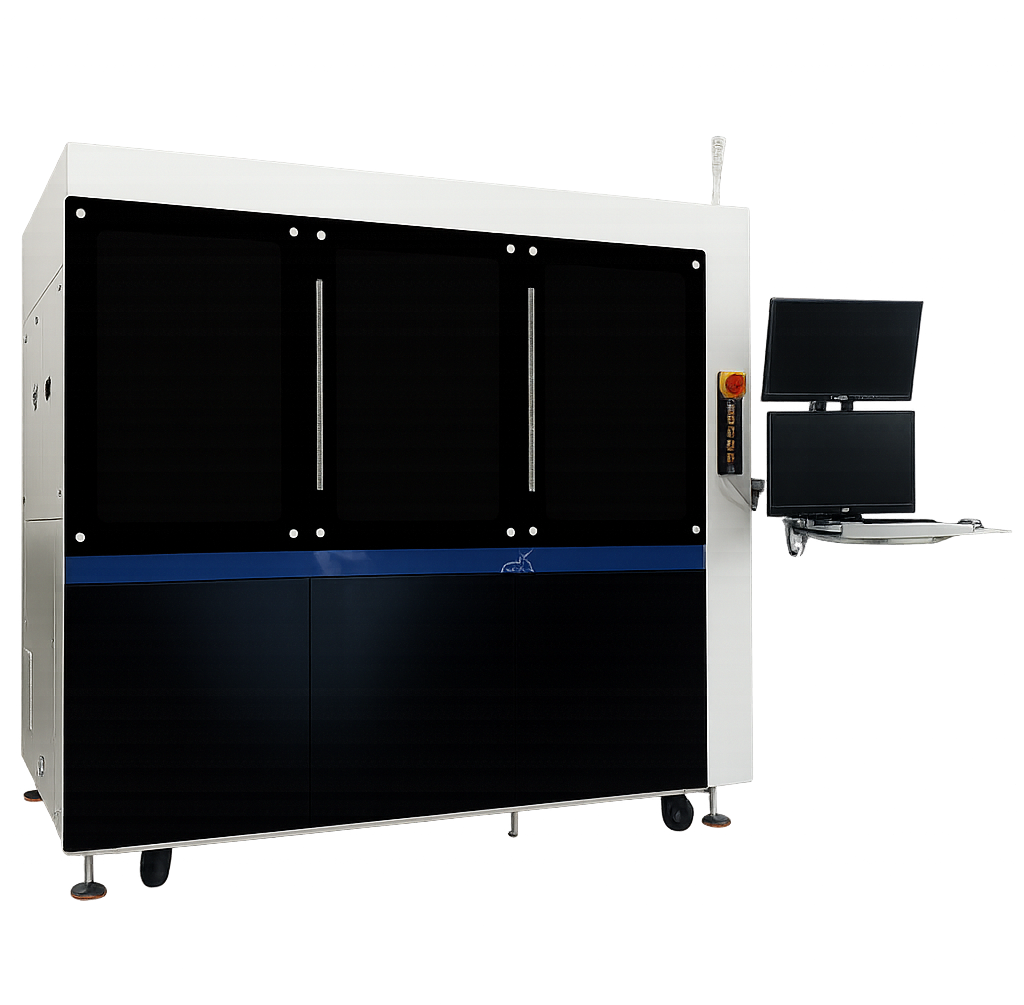
Laser Die Eutectic Bonding System
HP-EB3300- Features
- Supports multi-die and flip-chip eutectic bonding (including hybrid adhesive process)
- High-response heater with multi-stage PID and predictive control
- Real-time display of displacement, temperature, and pressure curves
- Dual bonding-table operation for high productivity
- Air-floating motion platform for long-term accuracy
- Rotatable dispensing system and adaptive bonding nozzle design
Description
The HP-EB3300 is a high-precision laser die eutectic bonding system designed for optoelectronic and semiconductor packaging. Featuring a dual bonding-table design, it supports single-die, flip-chip, and multi-die eutectic processes. Integrated with high-response temperature sensors and multi-stage PID control, it provides real-time monitoring of displacement, temperature, and pressure. The air-floating motion platform ensures long-term accuracy and stability.Specifications
| Bonding Method | High-precision bonding with feature side facing up (option: feature side facing down) | |
| Bonding Process | Eutectic bonding and silver-epoxy bonding | |
| Application |
|
|
| Placement Accuracy | ±1 μm (standard die); ±3 μm (depending on application) | |
| XY Motion (Loading/Unloading Platform) | Travel: 550 mm × 400 mm; Repeatability: 2.0 μm | |
| XY Motion (Bonding Axis Stage) | Travel: 250 mm × 100 mm; Repeatability: 0.5 μm | |
| Rotation Axis | Travel: 0° – 200°; Repeatability: 0.036° | |
| Bonding Force |
|
|
| Productivity | 25 s – 32 s(per device, depending on applicatio) | |
| Bonding Area | 13.0 mm × 13.0 mm | |
| Chip | Size | Min: 0.15 mm × 0.2 mm; Max: 3.0 mm × 8.0 mm |
| Feeding Method |
|
|
| Substrate | Size |
|
| Feeding Method |
|
|
| Weight | Approx. 2000 kg | |
| Ambient Temperature | Room temp. 22 °C ± 2 °C | |
| Humidity |
|
|